
A pair of Cockrell School research teams are part of a massive semiconductor grant program from the National Science Foundation that includes funds from industry leaders and the federal CHIPS Act.
The projects are part of the NSF Future of Semiconductors (FuSe) program through a public-private partnership between NSF and four major tech companies: Ericsson, IBM, Intel and Samsung. FuSe aims to enable rapid progress in new semiconductor technologies and manufacturing as well as workforce development.
Altogether, the program will support 24 research and education projects through 61 awards to 47 institutions totaling $45.6 million.
"The significance of semiconductor research in the technological landscape cannot be overstated," said Diana Marculescu, department chair in the Cockrell School of Engineering's Chandra Family Department of Electrical and Computer Engineering. "These NSF FuSe awards mark an initial step towards positioning us as a leading global institution in semiconductor research under the CHIPS Act."
The Projects: Li Shi, professor in the Walker Department of Mechanical Engineering, and electrical and computer engineering professor Xiuling Li are leading a project focused on heterogeneous integration of two types of semiconductors, gallium nitride and boron arsenide. Boron arsenide conducts heat much more efficiently than current-generation materials and can help to prevent overheating of operating devices. This team, which also includes researchers from The University of Texas at Dallas, University of Michigan-Ann Arbor, and The Ohio State University, aims to enhance performance and energy efficiency of semiconductor devices. The project also includes workforce training components, such as course materials and new courses on semiconductor materials and devices, annual Semiconductor Day with Industry, and Woman in Semiconductors Club, to provide training to students from diverse background and prepare them for the future-generation workforce of the semiconductor industry.
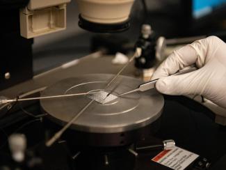
Working with researchers at Washington University in St. Louis, Massachusetts Institute of Technology, University of California Los Angeles, electrical and computer engineering professor Deji Akinwande is developing a groundbreaking technique for next-generation semiconductor processors using ultra-thin, two-dimensional semiconductor materials. The work will advance semiconductor technologies, integrating materials research, electronic devices, and innovative circuitry, while also including educational components for students, workshops and collaborations with semiconductor companies.
Why It Matters: There is a significant push to improve semiconductor manufacturing, innovation and research in the U.S. in the wake of pandemic-era supply chain shortages that impacted everything from medical devices to automobiles. Additionally, researchers around the world are working to improve semiconductor capabilities to support next-generation technologies heavy on processing, such as artificial intelligence, autonomous vehicles and more.
Future semiconductors and microelectronics will require a broad coalition of science and engineering talent in academic and industrial sectors to pursue holistic, "co-design" approaches that advance materials, devices and systems integration. Co-design approaches simultaneously consider the performance, manufacturability, recyclability and environmental sustainability of such materials, devices, and systems.
"Our investment will help train the next generation of talent necessary to fill key openings in the semiconductor industry and grow our economy from the middle out and bottom up," said NSF Director Sethuraman Panchanathan. "By supporting novel, transdisciplinary research, we will enable breakthroughs in semiconductors and microelectronics and address the national need for a reliable, secure supply of innovative semiconductor technologies, systems and professionals."
